Introduction
Microcontrollers connect the world of software to the world of hardware. They allow developers to write software which interacts with the physical world in the same deterministic, cycle-accurate manner as digital logic. They occupy the bottom left corner of the price/performance space, outselling their more powerful brethren by a factor of ten to one. They are the workhorses that power the digital transformation of our world.
RP2040 is the debut microcontroller from Raspberry Pi. It brings out signature values of high performance, low cost, and ease of use to the microcontroller space.
RP2040 is a stateless device, with support for cached execute-in-place from external QSPI memory. This design decision allows us to choose the appropriate density of non-volatile storage for our application, and to benefit from the low pricing of commodity Flash parts.
The post-fix numeral on RP2040 comes from the following,
RP = Raspberry Pi
2 = Number of Cores
0 = Type of core (M0+)
4 = floor (log2(ram / 16k))
0 = floor (log2(nonvolatile / 16k))
Key Features
RP2040 is manufactured on a modern 40nm process node, delivering high performance, low dynamic power consumption, and low leakage, with a variety of low-power modes to support extended-duration operation on battery power.
The key features of RP2040 are:
• Dual ARM Cortex-M0+ @ 133MHz
• 264kB on-chip SRAM in six independent banks
• Support for up to 16MB of off-chip Flash memory via dedicated QSPI bus
• DMA controller
• Fully-connected AHB crossbar
• Interpolator and integer divider peripherals
• On-chip programmable LDO to generate core voltage
• 2 on-chip PLLs to generate USB and core clocks
• 30 GPIO pins, 4 of which can be used as analogue inputs
• Peripherals
- 2 UARTs
- 2 SPI controllers
- I2C controllers
- 16 PWM channels
- USB 1.1 controller and PHY, with host and device support
- 8 PIO state machines
Block Diagram
Figure 1: System Overview of RP2040
Code may be executed directly from external memory through a dedicated SPI,DSPI or QSPI interface. A small cache improves performance for typical applications.
Debug is available via the SWD interface.
Internal SRAM can contain code or data. It is addressed as a single 264 kB
region, but physically partitioned into 6
banks to allow simultaneous parallel access from different masters.
DMA bus masters are available to offload repetitive data transfer tasks from the
processors.
GPIO pins can be driven directly, or from a variety of dedicated logic functions.
Dedicated hardware for fixed functions such as SPI, I2C, UART,
Flexible configurable PIO controllers can be used to provide a wide variety of IO functions.
Four ADC inputs which are shared with GPIO pins.
Two PLLs to provide a fixed 48MHz clock for USB or ADC, and a flexible
system clock up to 133MHz.
An internal Voltage Regulator to supply the core voltage so the end product
only needs supply the IO voltage.
Pin Locations
The IC comes in QFN package and has total 56 pins of different functions. There are total 26 multifunctional GPIO pins, 2 SPI, 2 I2C, 2 UART, 3 × 12-bit ADC, 16 × controllable PWM channels and 8 Programmable I/O (PIO) state machines for custom peripheral support.

Figure 2: Pinout of RP2040
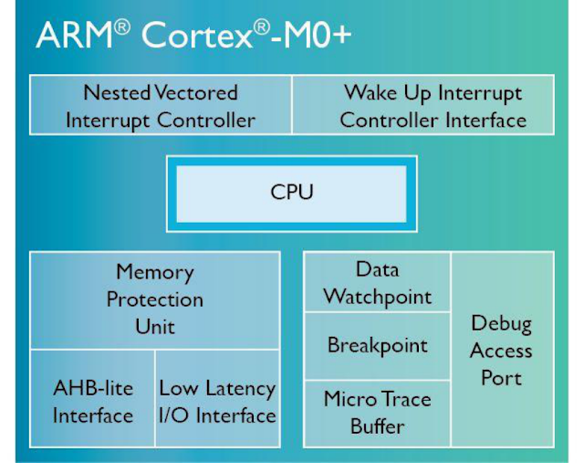
The Cortex M0+
The RP2040 is based on Arm Cortex M0+ architecture and is the most energy-efficient Arm processor available for constrained embedded applications. The Cortex-M0+ is successor of Cortex-M0 processor, The exceptionally small silicon area, low power and minimal code footprint of Cortex-M0+ enables
developers to achieve 32-bit performance at an 8-bit price point, bypassing the step to 16-bit devices. The Cortex-M0+ processor comes with a wide selection of options to provide flexible development.
Figure 3: ARM Cortex M0+ architecture
Memory of RP2040
RP2040 has embedded ROM and SRAM, and access to external Flash via a QSPI interface. Details of internal memory are given below.
• ROM
A 16kB read-only memory (ROM) is at address 0x00000000. The ROM contents are fixed at the time the silicon is manufactured. It contains:
1. Initial startup routine
2. Flash boot sequence
3. Flash programming routines
4. USB mass storage device with UF2 support
• SRAM
There is a total of 264kB of on-chip SRAM. Physically this is partitioned into six banks.There are no restrictions on what is stored in each bank: processor code, data buffers, or a mixture. There are four 16k x 32-bit banks (64kB each) and two 1k x 32-bit banks (4kB each)
SRAM is mapped to system addresses starting at 0x20000000
• FLASH
External Flash is accessed via the QSPI interface using the execute-in-place (XIP) hardware. This allows an external flash memory to be addressed and accessed by the system as though it were internal memory. Bus reads to a 16MB memory window starting at 0x10000000 are translated into a serial flash transfer, and the result is returned to the master that initiated the read.
Raspberry Pi Pico
Figure 4: Raspberry Pi Pico Microcontroller
Pico is a very first microcontroller based on RP2040 IC, designed by Raspberry Pi foundation. It supports both C/C++ platform and micro-Python for programming. It is faster than current leading Arduino Uno microcontroller by almost 8 times and faster than ESP32 by almost 1.5 times.


0 Comments